Circuit Intelligence -- LMM for PCB Design
Penn State University 2
Overview
PCB design is still a high-friction engineering workflow. A designer must translate product requirements into functional modules, search datasheets, choose ICs, create footprints, draw schematics, reason about nets, verify rules, simulate behavior, prepare layouts, and finally package BOM, Gerber, assembly, and 3D files for manufacturing. Small mistakes in pin geometry, connectivity, or design rules can trigger expensive respins.
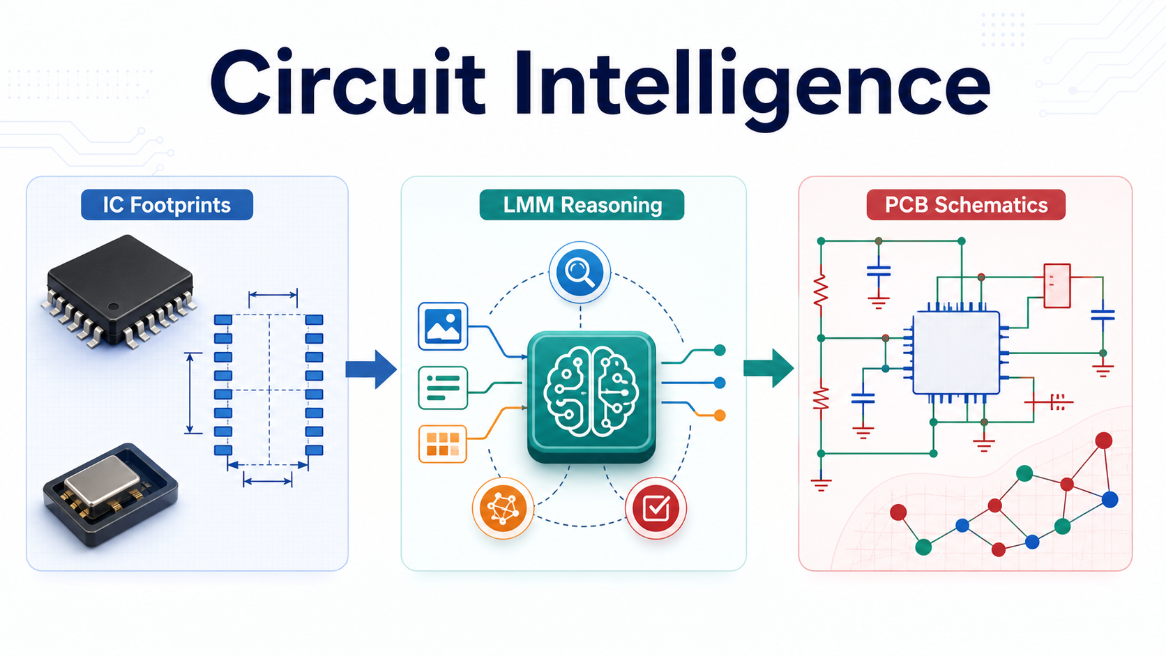
Circuit Intelligence is our vision for LMM for PCB Design: a domain-specific multimodal system that understands circuit artifacts as engineering documents, not ordinary pictures. The goal is to place natural language requirements, datasheets, package drawings, PCB schematics, layouts, BOMs, Gerbers, and production constraints into a shared semantic space where models and agents can reason, check, and generate verifiable design assets.
LMM4PCB Vision
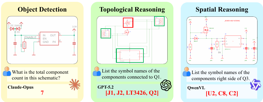
The LMM4PCB direction asks how a model can move from “reading” circuit diagrams to participating in an engineering workflow. A useful PCB model must parse requirements, retrieve device knowledge, understand geometry, recover schematic topology, reason about constraints, and expose uncertainty before its output enters an EDA or manufacturing flow.
Our work treats the platform as a closed loop rather than a single prediction task. Multimodal data and PCB knowledge bases provide the domain substrate. Specialized agents handle requirement parsing, footprint geometry, schematic graph reasoning, rule review, and EDA interaction. Structured outputs then return to simulation, prototype verification, and manufacturing feedback.
Technical Stack
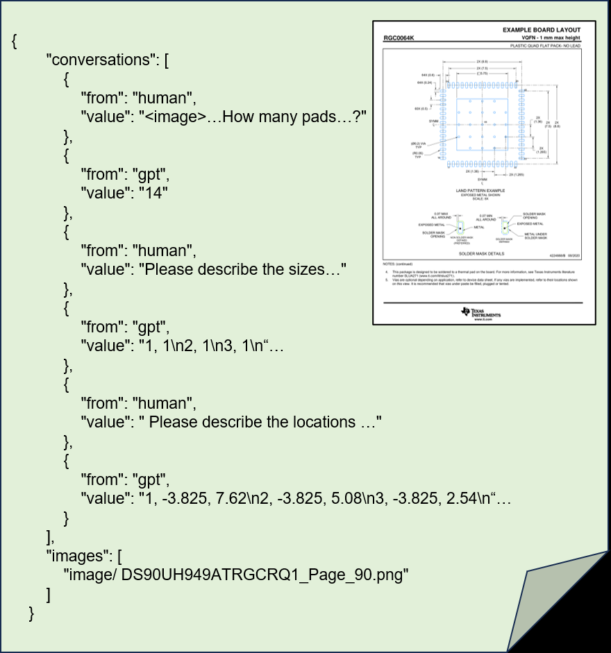
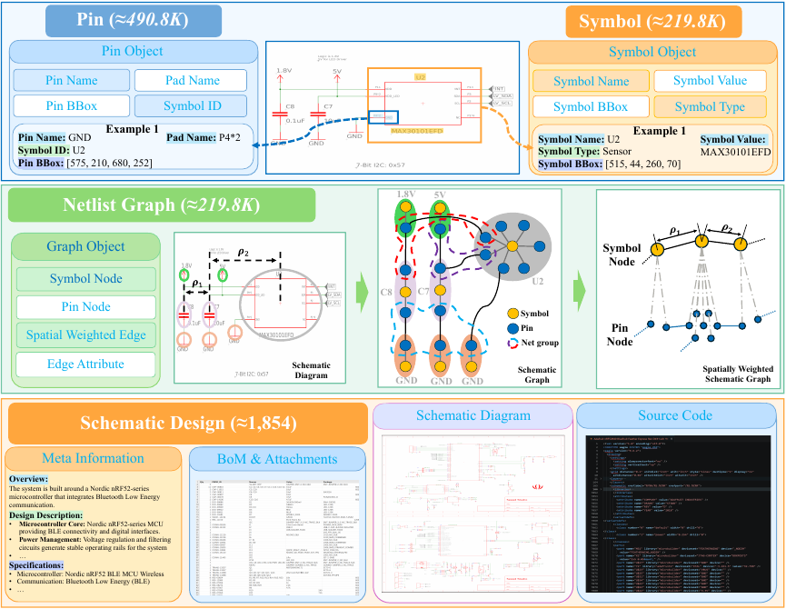
Engineering semantic layer. PCB artifacts are heterogeneous: text requirements, datasheet tables, package diagrams, schematic symbols, spatial layouts, BOM rows, and manufacturing rules. We organize them as linked multimodal objects so that models can reason over geometry, topology, text, and constraints together.
Agentic design workflow. The system decomposes PCB work into auditable steps: requirement understanding, IC selection, package and pin extraction, schematic graph construction, rule checking, simulation support, layout suggestion, and production-file preparation. Agents are useful here because each step has different evidence, failure modes, and verification criteria.
Design-to-manufacturing loop. A PCB assistant is only useful if its outputs survive real engineering checks. The workflow therefore emphasizes structured artifacts, EDA importability, ERC/DRC-style validation, prototype feedback, and manufacturing constraints instead of free-form diagram descriptions.
Research Foundation
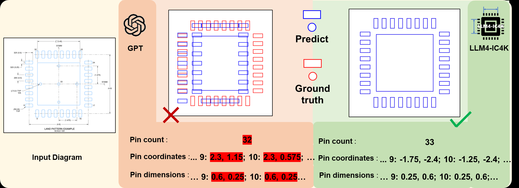
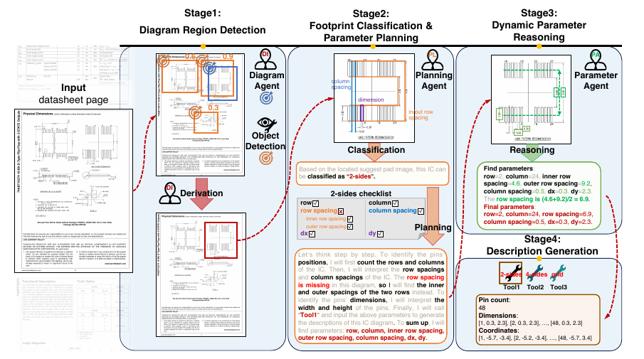
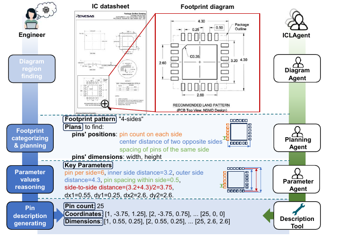
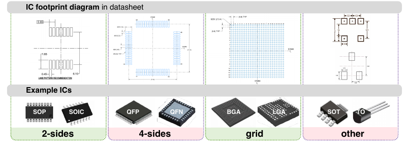
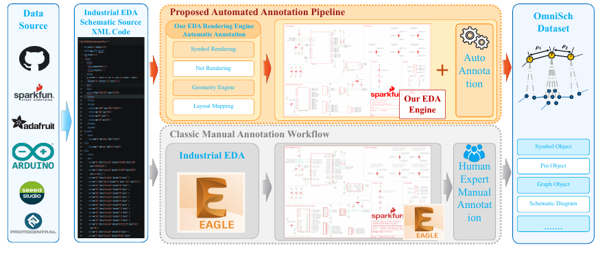
The publications below contribute core capabilities to this larger direction. They establish datasets and reasoning tasks for IC footprint geometry, multi-agent footprint labeling, and PCB schematic graph understanding. Together, these results form a research base for moving from visual circuit understanding toward practical PCB design automation.
Why It Matters
The long-term opportunity is not just faster annotation or better diagram QA. It is a new interface for hardware design: a system where engineers can state intent, inspect model evidence, revise constraints, and receive machine-checkable circuit assets that remain compatible with existing EDA and manufacturing pipelines.
This can lower the barrier to PCB design for small teams, reduce avoidable footprint and connectivity errors, shorten design-to-prototype cycles, and build reusable design knowledge for intelligent EDA and electronics manufacturing.